
In the ever-evolving landscape of technology, printed circuit boards (PCBs) stand as the backbone of innovation. From the simplest electronic gadgets to the most complex machinery, PCBs form the intricate web of connections that bring functionality to life. At eRio Circuits, we’re not just manufacturers; we’re architects of possibility, specializing in the design and fabrication of PCBs that push the boundaries of what’s achievable. Join us as we embark on a journey through the fascinating world of PCB design, focusing on the nuances of multi-layer and High-Density Interconnect (HDI) PCBs.
Understanding Multi-Layer PCBs: Unveiling the Layers of Complexity
Traditional PCBs consist of a single layer of conductive material sandwiched between insulating layers. However, as the demand for smaller, more powerful devices grows, so does the need for PCBs with increased functionality and efficiency. Enter multi-layer PCBs, the epitome of complexity in circuit board design.
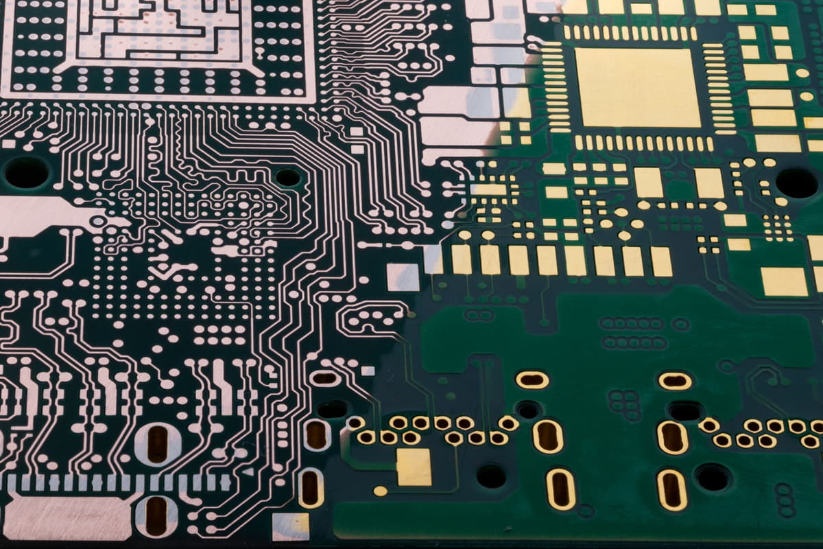
Multi-layer PCBs feature multiple layers of conductive material interconnected by insulating layers, allowing for a higher density of components and more intricate circuitry. At eRio Circuits, we specialize in the layout design of multi-layer PCBs, scaling up to a staggering 16 layers. This capability enables us to accommodate the most demanding design requirements, from high-performance computing systems to advanced telecommunications equipment.
Navigating the Complexity: Layout Design of Multi-Layer PCBs
The layout design of multi-layer PCBs is a meticulous process that requires careful consideration of factors such as signal integrity, thermal management, and manufacturability. Our team of experienced engineers leverages state-of-the-art design tools and industry best practices to ensure optimal performance and reliability.
From component placement to routing, every aspect of the layout is meticulously scrutinized to minimize signal interference and optimize signal integrity. Advanced techniques such as controlled impedance routing and differential pair routing are employed to meet the stringent requirements of high-speed digital and analog circuits.
Moreover, our expertise extends beyond the design phase to encompass manufacturability. By adhering to design for manufacturability (DFM) guidelines, we ensure seamless transition from prototype to production, minimizing time-to-market and reducing overall costs.
Unlocking the Potential: High-Density Interconnect (HDI) PCBs
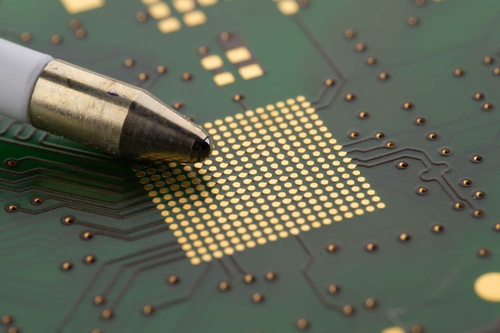
In today’s fast-paced world, miniaturization is key. HDI PCBs represent the pinnacle of miniaturization, offering unmatched density and functionality in a compact form factor. These specialized PCBs feature microvias, buried vias, and sequential lamination techniques, allowing for the interconnection of densely packed components with precision and reliability.
At eRio Circuits, we excel in the design and fabrication of HDI PCBs, leveraging our expertise to push the boundaries of what’s possible. Whether it’s a smartphone, a wearable device, or a medical implant, our HDI PCBs enable the realization of innovative products that redefine the limits of technology.
Conclusion: Empowering Innovation, One Circuit at a Time
Innovation knows no bounds, and neither do we. At eRio Circuits, we’re committed to empowering innovators with cutting-edge PCB design solutions that propel their ideas to new heights. Whether you’re a seasoned engineer, a budding entrepreneur, or a student exploring the realms of technology, we’re here to support you every step of the way.
From the layout design of multi-layer PCBs to the intricacies of HDI technology, we bring passion, expertise, and dedication to every project we undertake. Join us on this journey of discovery and innovation, and together, let’s shape the future of technology.
For all your PCB design needs, trust eRio Circuits to be your partner in innovation. Contact us today to learn more about our comprehensive range of services.