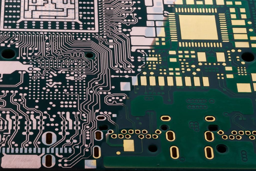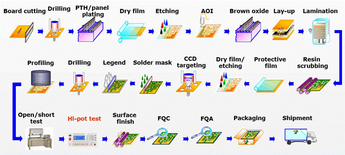
Printed Circuit Boards (PCBs) are the backbone of modern electronics, serving as the platform for connecting and supporting electronic components. The PCB manufacturing process involves several intricate steps to ensure the creation of high-quality boards that meet the specific requirements of the intended application. Below is a comprehensive overview of the PCB manufacturing process:
Designing the PCB:
- The process begins with the design of the PCB using specialized software. Designers lay out the circuitry, determine the placement of components, and define the connections between them. This design file serves as the blueprint for the entire manufacturing process.
Gerber File Generation:
- Once the design is complete, Gerber files are generated. These files contain the necessary information regarding the layout, traces, pads, and other features of the PCB. Gerber files are essential for the fabrication and assembly stages.
Material Selection:
- The choice of materials for the PCB depends on factors such as the intended application, environmental conditions, and cost considerations. Common materials include fiberglass-reinforced epoxy resin for the substrate and copper for the conductive traces.
Substrate Preparation:
- The substrate material, typically a thin layer of fiberglass, is cleaned and prepared for the next steps. This may involve cutting the substrate to the required size and applying a layer of copper foil to one or both sides.
Printing the Circuit:
- Using the Gerber files as a guide, the circuit pattern is printed onto the substrate. This can be done using various techniques such as etching, screen printing, or photolithography. The goal is to transfer the circuit pattern onto the copper foil layer accurately.
Etching:
- Etching is the process of removing excess copper from the substrate, leaving behind only the desired circuit traces. This is typically achieved by immersing the printed board in an etchant solution that selectively dissolves the unprotected copper.
Drilling:
- Holes are drilled into the board to accommodate the insertion of electronic components and to establish electrical connections between different layers of the PCB. High-precision drilling machines are used to ensure accuracy and consistency.
Plating:
- Plating is carried out to reinforce the circuit traces and provide a more durable surface finish. This involves electroplating the board with a thin layer of metal, usually tin or gold, to protect the copper traces from oxidation and corrosion.
Solder Mask Application:
- A solder mask is applied over the entire surface of the PCB, leaving only the areas where components will be soldered exposed. The solder mask helps prevent solder bridges and ensures proper soldering during assembly.
Silkscreen Printing:
- Identifying information such as component labels, polarity markers, and company logos are printed onto the PCB using a silkscreening process. This information assists in the assembly and troubleshooting of the final product.
Testing and Quality Control:
- Before proceeding to assembly, the PCB undergoes rigorous testing to ensure that all connections are intact, and there are no defects in the circuitry. Automated testing equipment is used to check for continuity, shorts, and other issues.
Final Assembly:
- Once the PCB passes testing, it is ready for final assembly. Electronic components such as resistors, capacitors, integrated circuits, and connectors are soldered onto the board using automated pick-and-place machines or by hand for specialized components.
Final Inspection:
- The assembled PCB undergoes a final inspection to verify the correct placement and soldering of components. Visual inspection and functional testing may be performed to ensure that the PCB meets the specified requirements.
Packaging and Shipping:
- Once the PCBs pass inspection, they are packaged according to customer requirements and prepared for shipping. Proper packaging is essential to protect the boards during transit and storage until they are ready for use.
In conclusion, the PCB manufacturing process is a complex series of steps that require precision, attention to detail, and adherence to strict quality standards. From initial design to final assembly, each stage plays a crucial role in producing high-quality PCBs that form the foundation of countless electronic devices used in various industries worldwide.